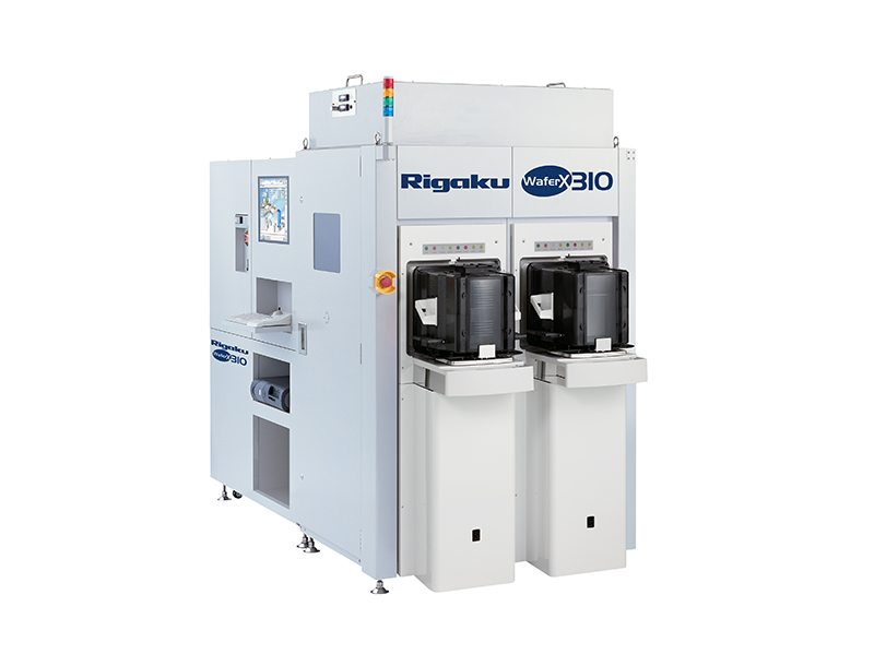
WAFERX 310
Wavelength-Dispersive X-ray Fluorescence simultaneous spectrometer
IN-LINE, SIMULTANEOUS WD-XRF SPECTROMETER FOR HIGH-VOLUME SEMICONDUCTOR MANUFACTURING
Technical SPECIFICATIONS
Rigaku's WaferX 310 represents the culmination of more than 40 years of experience in the X-ray fluorescence analysis of thin films on silicon wafers. Developed as an in-line metrology tool, it is ideally suited to 300 mm high-volume manufacturing environments.
Simultaneous thickness and composition
The WaferX 310 is ideal for measuring BPSG, PSG, and metal films. In addition, multi-layered film stacks, WSix, electrode films, ferrodielectric thin films, FRAM, next-generation DRAM, and SiOF are standard applications for this tool.
Analysis to support sub-micron technology
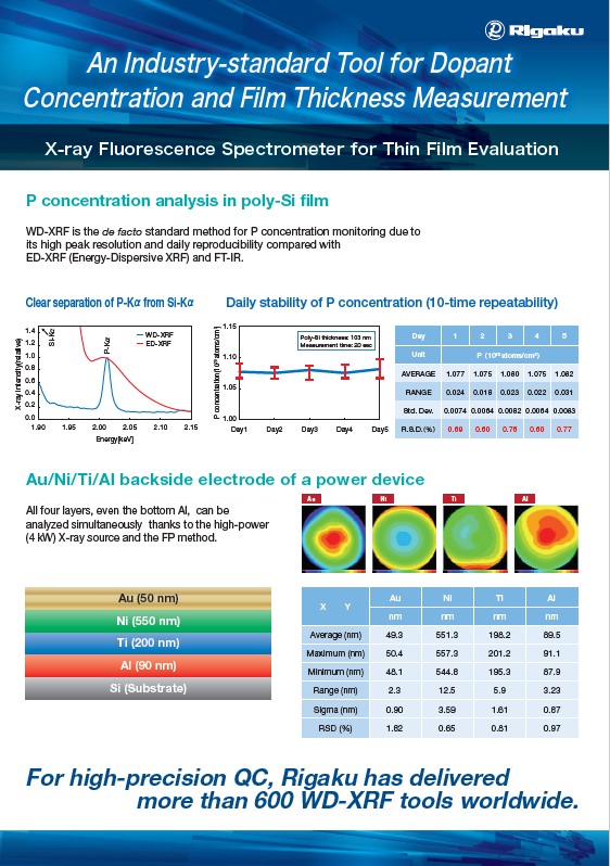
Highly accurate analyses for the ultra-light elements such as B and P in BPSG films have been improved significantly by employing a 4 kW high-power X-ray tube with a thin beryllium window.
Advanced design
The instrument employs a wafer height adjustment mechanism to compensate for differences in wafer thickness and a diffraction avoidance mechanism to eliminate diffraction interference for the transition metals.
- Integrated FOUP (SMIF) is available, supporting the C-to-C standard.
- Various user cassettes can also be loaded. FOUP (SMIF) through-the-wall option is available.
- Wafers smaller than 300 mm can be measured using third-party FOUP adapters.
Software redesign
- 3D graphics display enables the operator to judge status clearly.
- The alarm position is displayed graphically, and accurate maintenance information is
- “Bubble chart” display enables the operator to easily judge the distribution of intensity on a
- More flexible parameter setting to avoid X-ray diffraction effects.
FEATURES & BENEFITS
- Patented "diffraction avoidance" capability for accurate XRF results
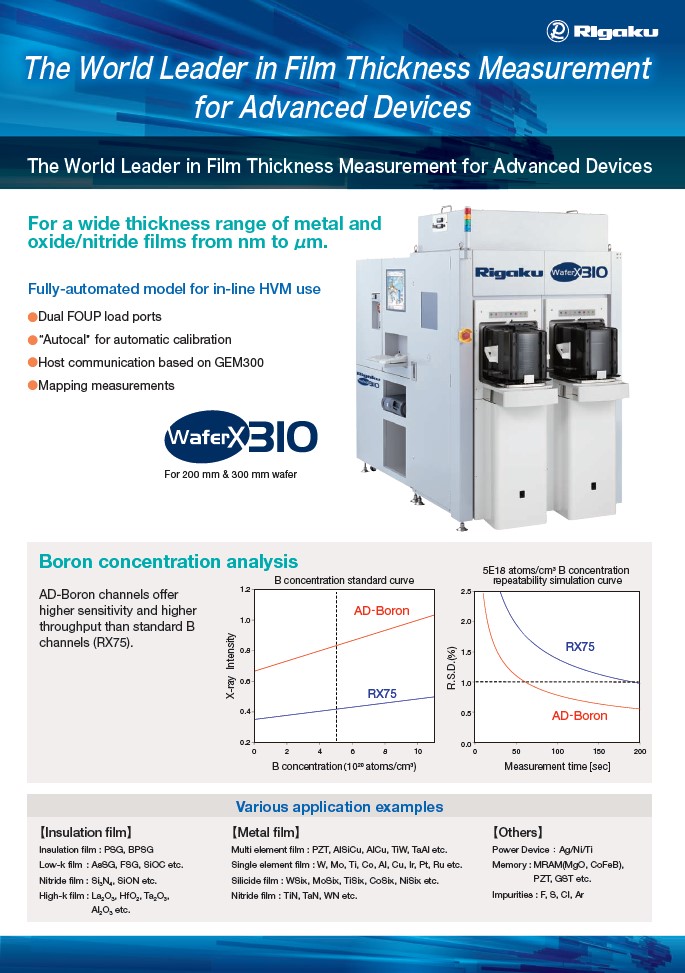
- High-sensitivity Boron analysis (with AD-Boron channel)
- Robotic wafer handling and fully automated operation
- Solid-state, oil-free X-ray generator
- FOUP, SMIF, and through-the-wall configurations are available to meet the various needs of
- GEM300 Software
- Auto Calibration
- SEMI S2/S8 Compliance
SYSTEM PARAMETERS |
SPECIFICATIONS |
|
Metrology Tool |
WaferX 310 |
|
Technique |
Simultaneous wavelength-dispersive X-ray fluorescence |
|
Benefit |
Thickness and composition of multi-layer stacks for 300 mm, and 200 mm wafers |
|
Technology |
Process WD-XRF with 4 kW, Rh-anode source and factory automation core |
|
Core attributes |
20 channels max., fixed type (₄Be ~₉₂U), scanning type (₂₂Ti ~₉₂U), CE marked, GEM300, SEMI S2/S8 |
|
Core options |
Available with 300 mm factory automation, 2 available FOUP (SMIF) load ports, AD-Boron channel |
|
Computer |
Internal PC, MS Windows® OS |
|
Core dimensions |
1200 (W) x 1950 (H) x 2498 (D) mm |
|
Mass |
1166 kg (core unit) |
|
Power requirements |
3Ø, 200 VAC 50/60 Hz, 50 A |
MEASURABLE ELEMENTS
QUANTITATIVE METHOD
ANALYZABLE STRUCTURE
ANALYZABLE THICKNESS
Be - U
WD-XRF can measure ultra-light elements, such as B, C, N, O.
Mg and Al are also easy to measure due to the high resolution of WD-XRF.Advanced FP Method
FP (Fundamental Parameters) method enables thickness and composition analysis with one recipe.
Up to 20 stacked layers can be analyzed.
The FP method can calculate the absorption effect from other layers. Therefore, analyses of compound films or multi-layers are the strong point of WD-XRF.Sub-angstrom (Å) to micrometer (μm) levels
Rigaku WD-XRF employs high-power
X-ray tubes 4 kW enabling the measurement of
ultra-thin films.
APPLICATIONS
XRF APPLICATIONS FOR THIN FILMS
FRONT-END SEMICONDUCTOR manufacturing
BACK-END SEMICONDUCTOR manufacturing
| Semiconductor Film |
Doped poly-Si (B, P, C, N, As), SiGe (...) |
| Insulation film |
Insulator film, Low-k film, Nitride film, and High-k film. (...) |
| Metal Conductive Film |
Metal alloy film, Silicide film, and Nitride film (...) |
| Power Device |
|
| Memory Device |
MRAM (MgO, CoFeB), GST, BST, SBT, (...) |
| SnAg Solder Bump |
IGZO, CIGS, Ar (Inert gas), C, Cl, (...) |
| Oxide Films | SiO2, (...) |
| Ion Implant Dose | P, As, (...) |
| Gate Dielectric | HfSiON, Al2O3, (...) |
| Gate Electrode | WSix, poly-Si, SiGe, (...) |
| Salicide | CoSi, NiSi, (...) |
| Contact Plug | W, poly-Si, (...) |
| Capacitor Electrode | TaAl, Ir, Pt, (...) |
| Capacitor Insulator | Ta2O5, BST, (...) |
| Inter-layer Dielectric | PSG, BPSG, FSG, SiOC, (...) |
| Barrier Metal | Ta, TaN, WN, Ti, TiN, (...) |
| Interconnect Metal | Cu (Seed & ECD), AlSiCu, (...) |
| Etch Stop Layer | Si3N4, SiC, (...) |
| Back-side Metallization | Ti, Al, Ni, Ag, Au, (...) |
WAFERX 310 RESOURCES
TRUSTED PARTNER
Pharmaceuticals have the power to change the world for the better, but before they can ever do that, they need to be proven safe and trustworthy. Here at Rigaku, we strive to make this a reality as the leading global scientific analytical instrumentation company specializing in X-ray and thermal analysis, and Raman spectroscopy.
CORPORATE MISSION
To contribute to the enhancement of humanity through scientific and technological development.
CORPORATE MOTTO
Value our customers, value our people, and value our technology


