ED-XRF, XRR and OPTICAL METROLOGY TOOLS
Hybrid Wafer Metrology
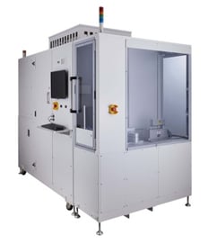
ONYX 3000Micro-spot ED-XRF and Optical Inspection (2D-3D)
In-line non-destructive inspection and metrology for the semiconductor and micro-electronics industries ≤300 mm wafers |
xhemis® ex-2000ED-XRF and XRR for High-Volume Manufacturing
Thickness, density, roughness, and composition of films on blanket wafers metrology tool for blanket wafers ≤200 mm |
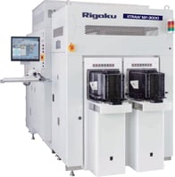
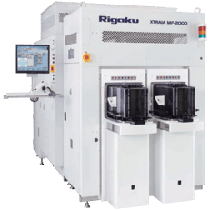
xTRAIA® MF-2000Process XRR, ED-XRF, and XRD Metrology Fab Tool
Blanket and patterned metal layer thickness and composition
|
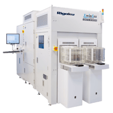
xTRAIA® MF-3000XRR, ED-XRF, XRD Metrology Optimized for High-Volume Manufacturing
Blanket and patterned metal layer thickness and composition
|
XRR: X-ray Reflective Spectrometer | Typically for characterization of a multilayered sample
ED-XRF: Energy-dispersive X-ray fluorescence (ED-XRF) spectrometer
OPTICAL TOOLS: Hybrid wafer metrology combining micro-spot ED-XRF and 2D microscope, and 3D scanner for In-line non-destructive inspection and metrology.
HYBRID WAFER METROLOGY
Combining advanced X-ray and optical techniques, the ONYX 3000 offers a unique wafer metrology approach in many areas from FEOL through WLP, leading to in-line solutions for these processes. This sophisticated hybrid metrology tool enables high-throughput, in-line measurements on a blanket and product wafers ranging from ultra-thin single-layer films to multi-layer stacks.Who we are
Rigaku Semiconductor Metrology Division
Semiconductors have the power to change the world for the better. Here at Rigaku, we strive to make this a reality as the leading global supplier of X-ray metrology tools for semiconductor process R&D and high-volume manufacturing.
To contribute to the enhancement of humanity through scientific and technological development.
Value our customers, value our people, and value our technology.