Rigaku Logo 100px
1417705_RSMDSemiconductorIcons_11_072122

WD-XRF APPLICATION

 THICKNESS CHARACTERIZATION OF A POWER DEVICE

BACKSIDE ELECTRODE

WD-XRF can monitor metal film thickness and uniformity with high precision and throughput.


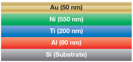
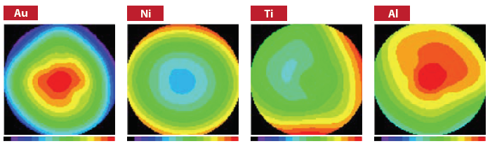
All four layers, even the bottom Al, can be analyzed simultaneously thanks to the high-power (4 kW) X-ray source and the FP method.

elements measeured by wd-xrf


X                     Y Au Ni Ti Al
nm nm nm nm
Average (nm) 49.3 551.3 198.2 89.5
Maximun (nm) 50.4 557.3 201.2 91.1
Minimun (nm) 48.1 544.8 195.3 87.9
Range (nm) 2.3 12.5 5.9 3.23
Sigma (nm) 0.90 3.59 1.61 0.87
RSD (%) 1.82 0.65 0.81 0.97


RECOMMENDED RIGAKU SEMICONDUCTOR METROLOGY TOOLS

AZX 400 Transparent Bcakground
Image - WDA-3650 - without autoloader 800x610
Image - WaferX 310 - 2018-11-21 800x610

AZX 400

Sequential WDXRF spectrometer for elemental analysis and thin-film metrology of large and/or heavy samples

WDA-3650

Simultaneous WDXRF spectrometer for wafer metal film metrology; up to 200 mm wafers

WAFERX 310

In-line, simultaneous WDXRF spectrometer for wafer metal film metrology; up to 300 mm wafers

Explore AZX 400
Explore WDA-3650
Explore WaferX 310