HYBRID METROLOGY
BUMP INSPECTION - COMPOSITION AND HEIGHT
The hybrid solution provides quick and reliable location of bump and wafer defects
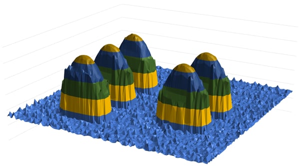
The hybrid solution provides a quick and reliable location of bump and wafer defects. The bump, a dome-like structure made of solderable material, is a crucial interconnecting element for connecting chips in a three-dimensional stack and for connecting the stack to the printed circuit board.
- Elemental composition analysis by optical analysis for geometrical parameters and XRF
- Vertical incident X-Ray beam (spot down to 7 µm on Sn K line) using four independent detectors configured in a symmetric assembly
- Thickness/composition extraction using robust Fundamental Parameters (FP) algorithm
- Composition analysis using Standardless Fundamental Parameter (SLFP) option

RECOMMENDED RIGAKU SEMICONDUCTOR METROLOGY TOOLS

BUMP INSPECTION SYSTEM
≤ 300 mm Metrology Solutions
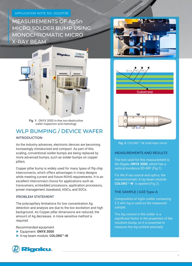
ONYX 3000 | Hybrid metrology, XRF and optical x-ray, with a 2D microscope, and 3D Scanner for blanket and patterned wafer thickness, composition, defect identification, and sizing
- Hybrid Configuration
- Micro-spot ED-XRF and 2D- and 3D- optical characterization of device structures
- For FEOL, BEOL, and packaging applications
- For up to 300 mm blanket and patterned wafers


