
Understanding Semiconductors | Episode 13
Understanding Semiconductors
Modern metrology from Lab to Fab by Rigaku.
A podcast for engineering leaders in characterization, metrology, process, and analytics, looking for discussion around semiconductor metrology challenges.
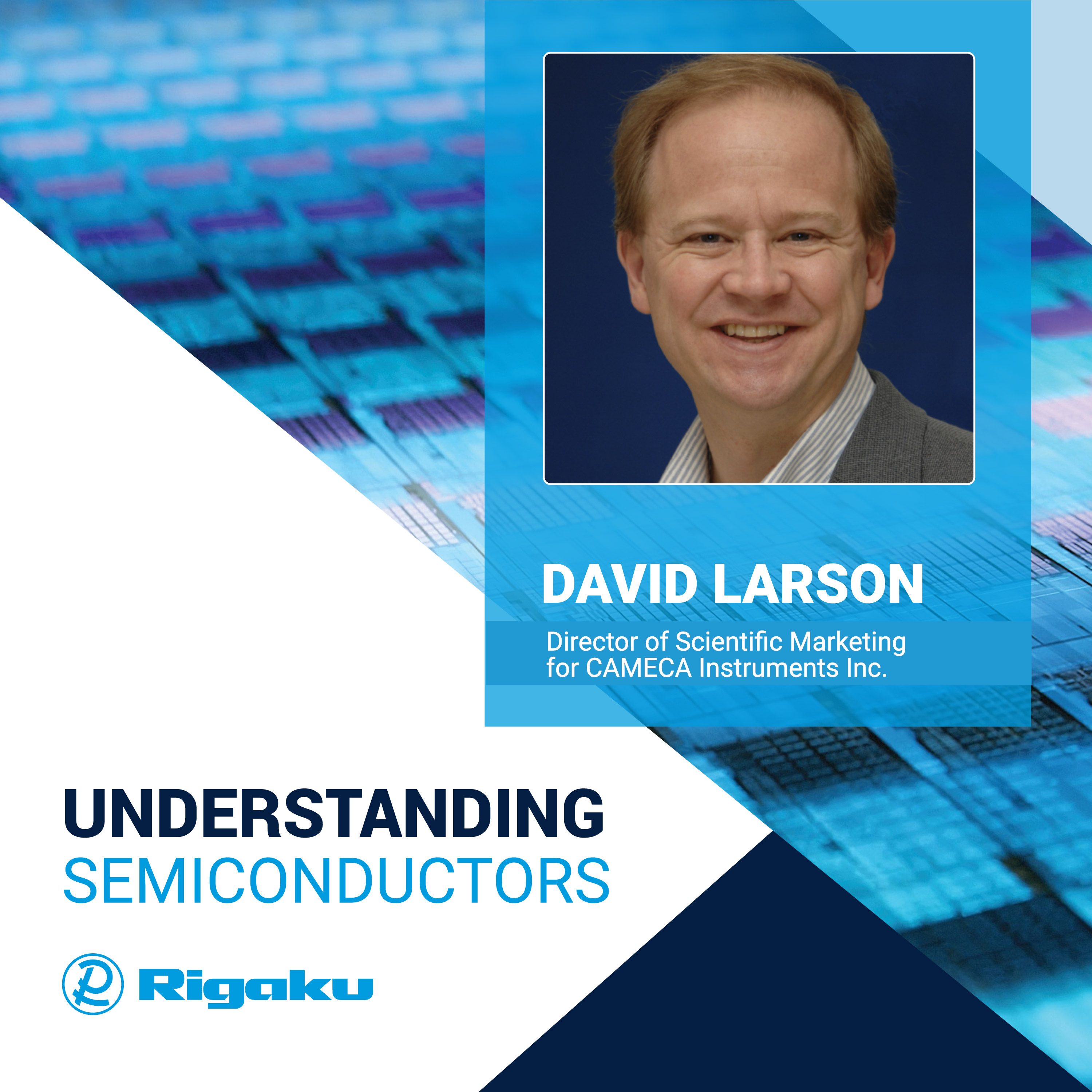
In this episode, Semiconductor Secrets Unveiled: Navigating Atom Probe Tomography with David LarsonEver wondered how atom probe tomography advances our understanding of semiconductors and improves device performance?
In today's episode, we dive deep into the world of semiconductors as we explore the fascinating realm of atom probe tomography. Our guest expert, David Larson, sheds light on the intricacies of this powerful materials characterization technique. From minimizing damage and improving yield to overcoming challenges in data reconstruction, David shares insights on the latest advancements and future possibilities in the field. Tune in to gain a deeper understanding of semiconductors and atom probe technology's role in their analysis.
Explore:
|
Visit our LinkedIn Semiconductor Metrology Solutions Showcase
Contact Markus Kuhn on LinkedIn for any potential guest requests or episode ideas.
To ensure you never miss an episode of the Understanding Semiconductor podcast, subscribe to Apple Podcasts, Spotify, Google, or our website. Listening on a desktop & can’t see the links? Just search for Understanding Semiconductors in your favorite podcast player.