Skip to content

2023 Semiconductor Forum Content Hub

Blog post primary image

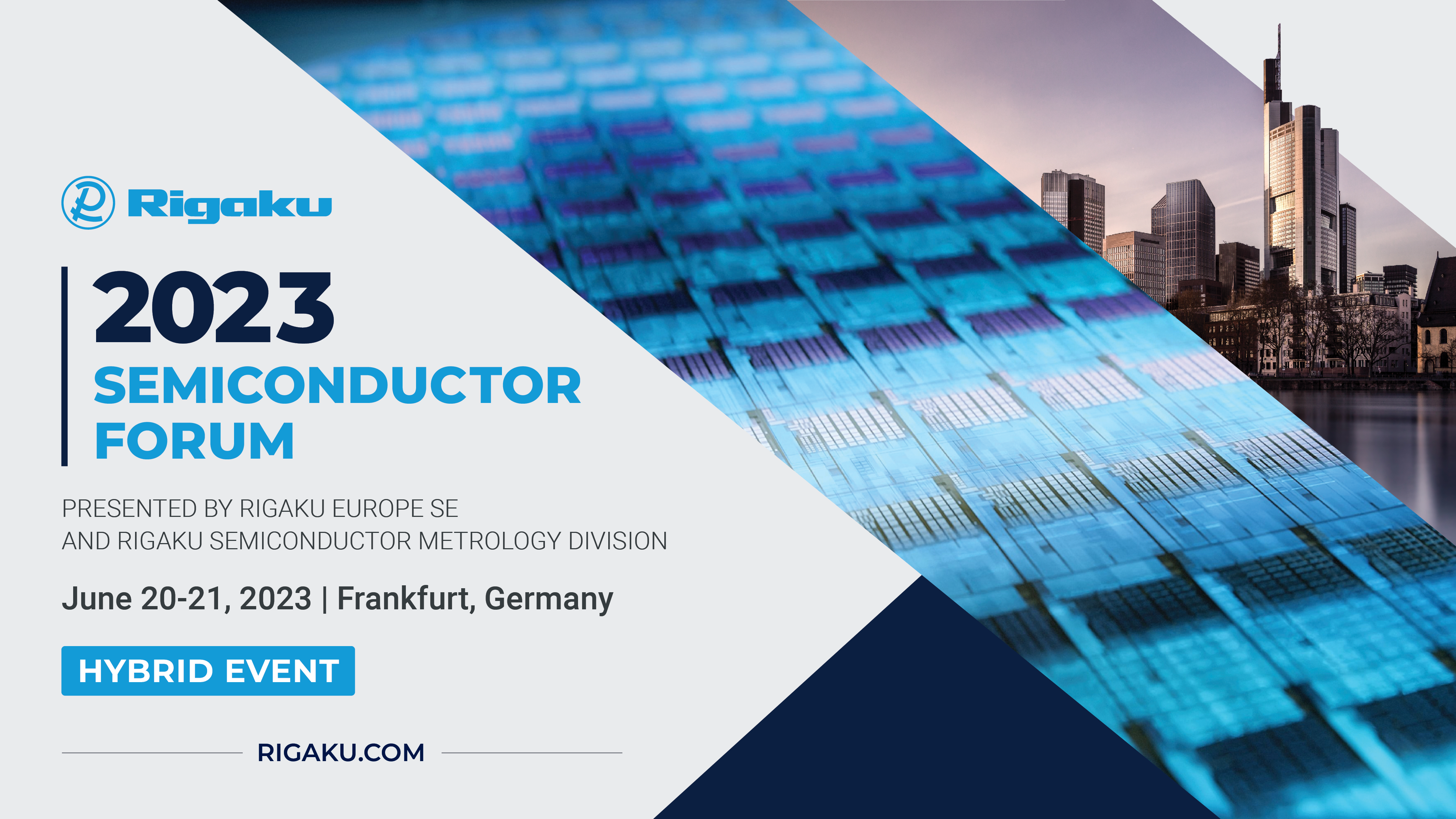
The World of Semiconductors Metrology Tools, from Lab to Fab

We thank everyone who attended our inaugural Rigaku Semiconductor Forum 2023. Our distinguished speakers provided valuable insights and perspectives, making the discussion informative and engaging. We thank all the participants who contributed to the success of our event.  We appreciate your participation in collectively driving progress in this critical field of study. We commend you for your support and active engagement throughout the forum; your expertise and dedication to advancing knowledge in the field of semiconductors have significantly contributed to the growth and vitality of our community.

Rigaku Europe SE and Rigaku Semiconductor Metrology Division brought this event to you.
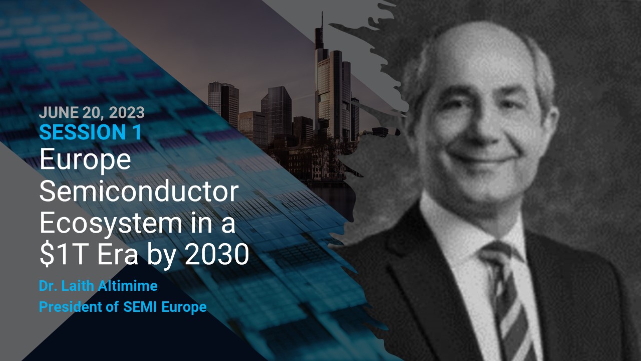
THE SESSIONS

Slide4

DAY ONE - SESSION 1


Europe Semiconductor Ecosystem in

a $1T Era by 2030

Dr. Laith Altimime - President of SEMI Europe

 VIEW PRESENTATION

Slide5

DAY ONE - SESSION 2


Metrology and Expectations

of tomorrow's IC Industry

Dr. Paul Van Der Heide - IMEC

 VIEW PRESENTATION

Slide6-1

DAY ONE - SESSION 3

Controlling Properties of

Wide Bandgap Materials in Industry

Dr. Andrea Severino -  ST Catania R&D ST Microelectronics

 VIEW PRESENTATION

Slide7

DAY ONE - SESSION 4

Third-generation photovoltaics

based on perovskites

Dr. Alessandra Alberti - National Research Council of Italy

 VIEW PRESENTATION

Slide8

DAY ONE - SESSION 5


An Introduction to
Nanovation and how we use XRD for

Characterization and Quality Control

of Oxide Semiconductors

Dr. David Rogers - Nanovation


Slide9

DAY TWO - SESSION 1


European Semi Outlook

Challenges and Opportunities


Boris Metodiev -TechInsights

VIEW PRESENTATION

Slide10

DAY TWO - SESSION 2


Integrated photonics

with Pockels materials

Dr. Jean Fompeyrine - Lumiphase


Slide11

DAY TWO - SESSION 3


X-ray Metrology Opportunities and Challenges

for Advanced Semiconductor Technologies

Dr. Kyioshi Ogata - Rigaku Corporation

Request information

Slide12

DAY TWO - SESSION 4

Metrology

from Lab to Fab

Dr. Abner Bello - Corning Incorporated

VIEW PRESENTATION

Slide13

DAY TWO - SESSION 5

Crystallographic defect characterization of semiconductor

single crystalline materials by X-ray topography

Dr. Ing. Christian Reimann - Fraunhofer

 VIEW PRESENTATION


IF YOU NEED MORE INFORMATION, CONTACT US AT:


RIGAKU EUROPE SE

Hugenottenallee 167

Neu-Isenburg

63263 , Germany

semieurope@rigaku.com

+49 6102 77999 51

RIGAKU AMERICAS CORPORATION

9009 New Trails Drive

The Woodlands, TX

77381-5209, USA

rsmd@rigaku.com

+1-281-362-2300

RIGAKU CORPORATION

3-9-12, Matsubara-cho

Akishima-shi, Tokyo

196-8666, Japan

info-gsm@rigaku.co.jp

+81 3-3479-0618