X-RAY MEASUREMENT SOLUTIONS FOR COMPOUND SEMICONDUCTORS

Compound Semiconductors
X-ray Metrology solutions for emerging power electronics devices, optoelectronics, 5G, and 6G communications.
SiC, GaN, GaAs, InP, Ga2O3
-
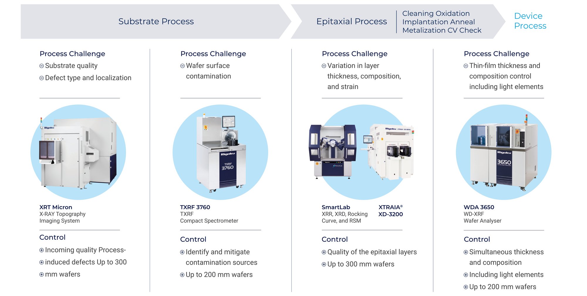
Surface Contamination Detection
-
Metrology of thin and ultra-thin films
-
Structure properties of epitaxial layers
-
Inspection of epitaxial substrate defects
-
Inspection of transparent wafers
-
Line process control
-
Data analysis
OUR SOLUTIONS
UPCOMING EVENTS

CS International 16th-17th APRIL 2024, BRUSSELS, BELGIUM

The 2024 International Conference on Frontiers of Characterization and Metrology for Nanoelectronics (FCMN) in Monterey, CA from April 15-18, 2024.
GET MORE INFORMATION ABOUT COMPOUND SEMICONDUCTOR METROLOGY AND INSPECTION SOLUTIONS
RECOMMENDED COMPOUND SEMICONDUCTOR METROLOGY TOOLS
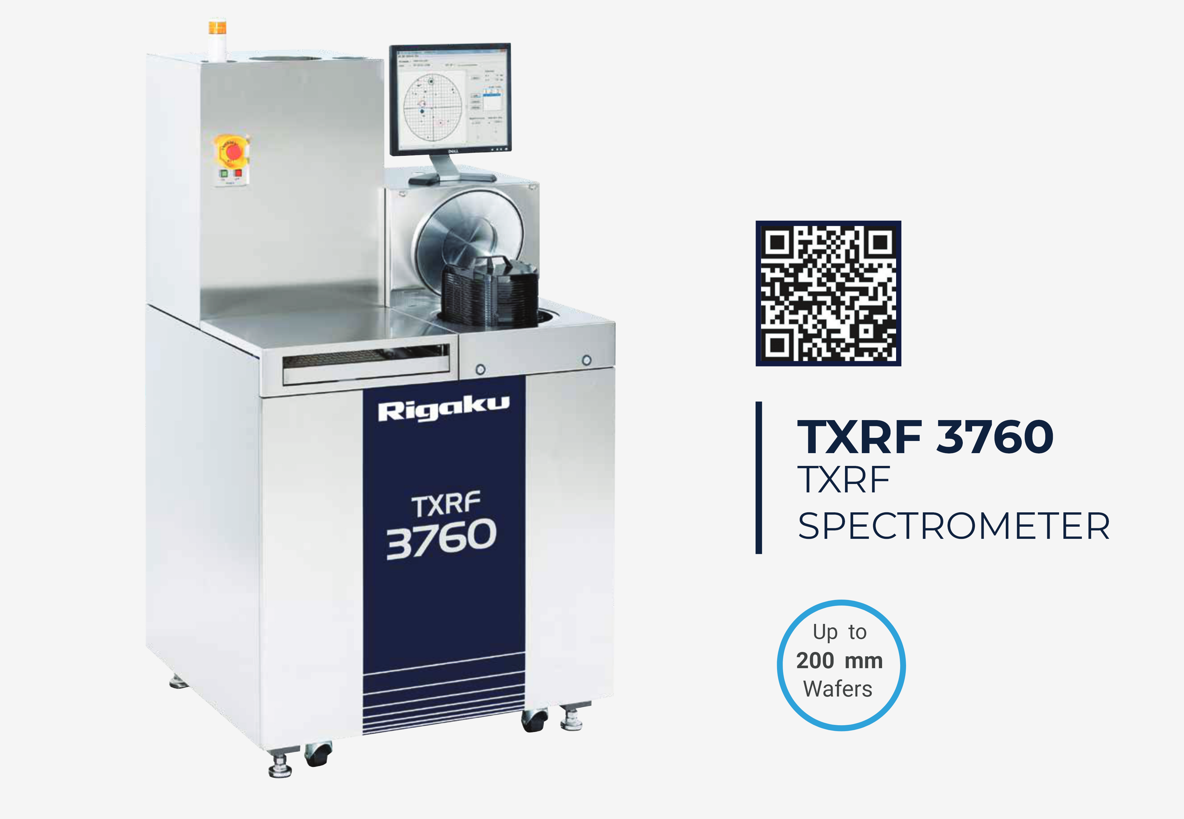
Wafer Surface Contamination Metrology With Light Elements Sensitivity
- Ease of operation and rapid analysis results
- Compact design, footprint <1 m2
- High-power rotating-anode source (9 kW)
- Liquid nitrogen-free detector (SDD)
- Three-beam excitation (W-M, W-Lb, H.E.)
- Wide range of analytical elements (Na~U)
- Light-element sensitivity (Na, Mg, Al)
- Application to bare Si, SiC, and non-Si substrate
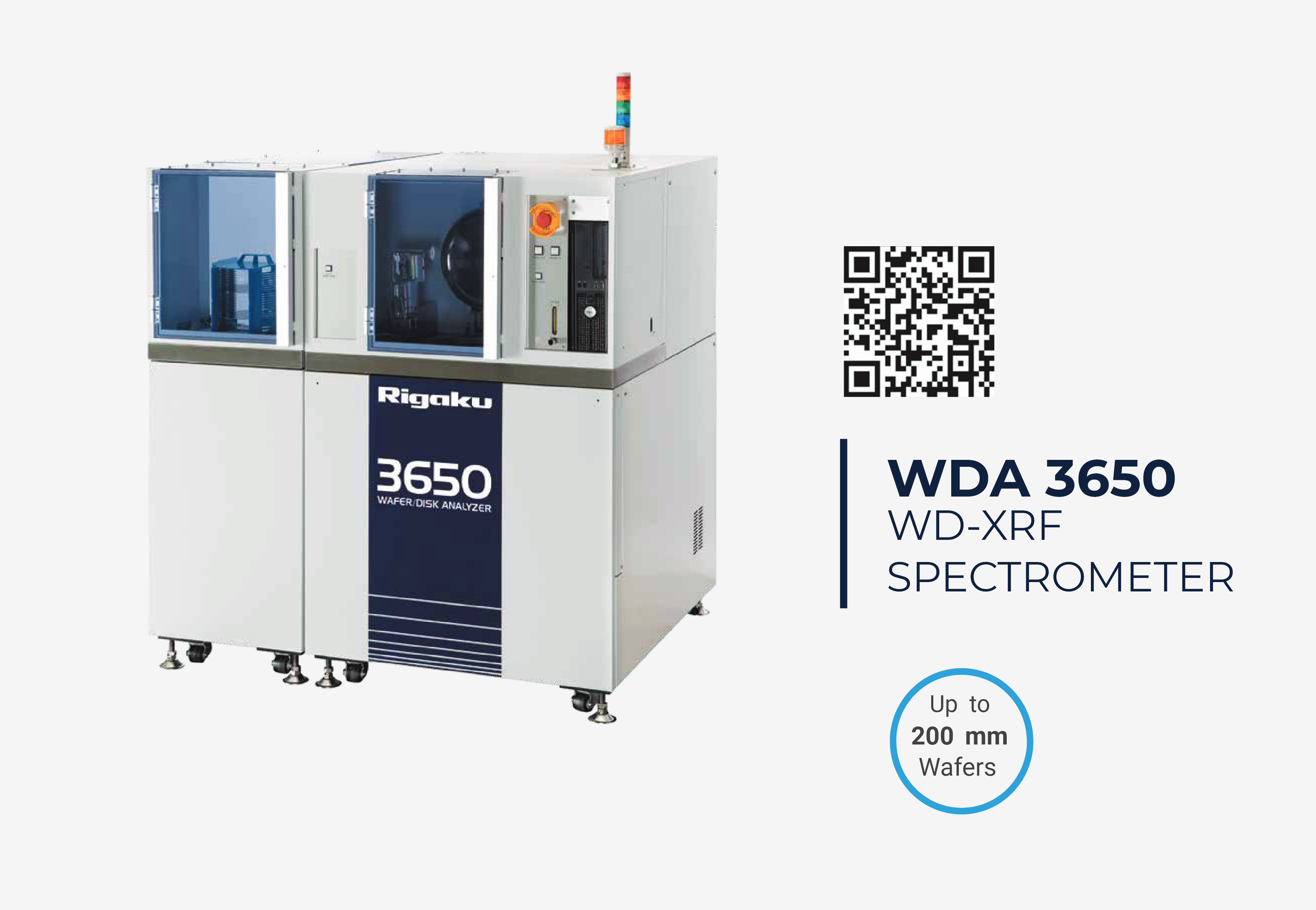
Simultaneous WDXRF spectrometer for film thickness and composition measurements on wafers
- Patented "diffraction avoidance" capability for accurate XRF results
- High-sensitivity Boron analysis (with AD-Boron channel)
- Solid-state, oil-free x-ray generator
- SMIF and through-the-wall configurations are available to meet the various needs of high-volume manufacturing wafer fabs
- Capable of high analytical performance, accuracy, and stability
- Simultaneous evaluation of film thickness and composition
- Applicable to all film types
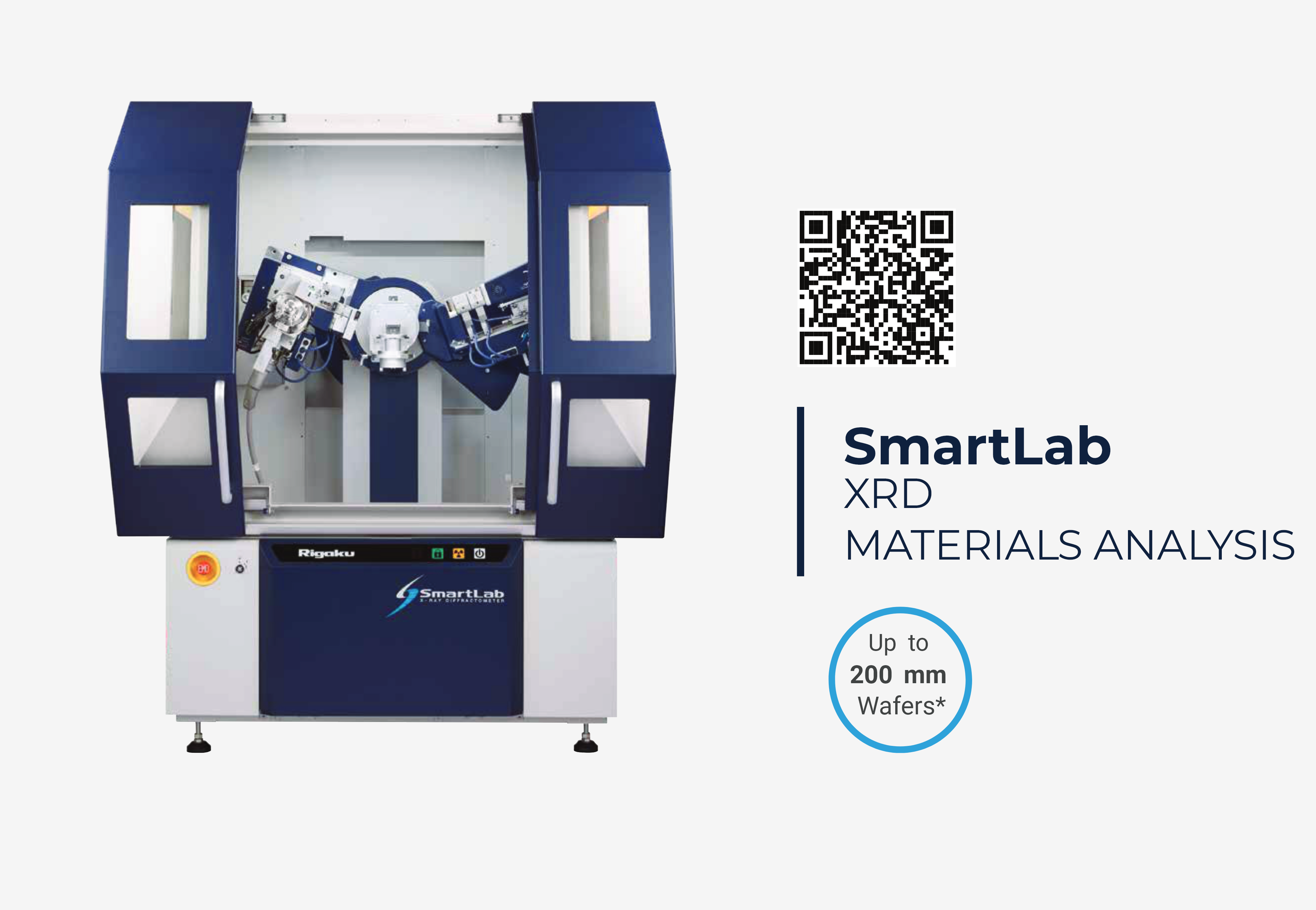
Automated Multipurpose X-Ray Diffractometer
- Available in-plane arm (5-axis goniometer)
- High-flux X-ray source: PhotonMax
- HyPix-3000 high energy resolution 2D HPAD detector
- New CBO family, with fully automated beam switchable CBO-Auto
- New CBO family, with high-resolution micro area CBO-μ
- Operando measurements with SmartLab Studio II software
- Multi-year component warranty contributes to the low cost of ownership
- Multiple sample stages to suit applications: Heating stages, 4-inch full map stage, 6-inch full map stage, and 2D reflection stage for GI SAXS/WAXS
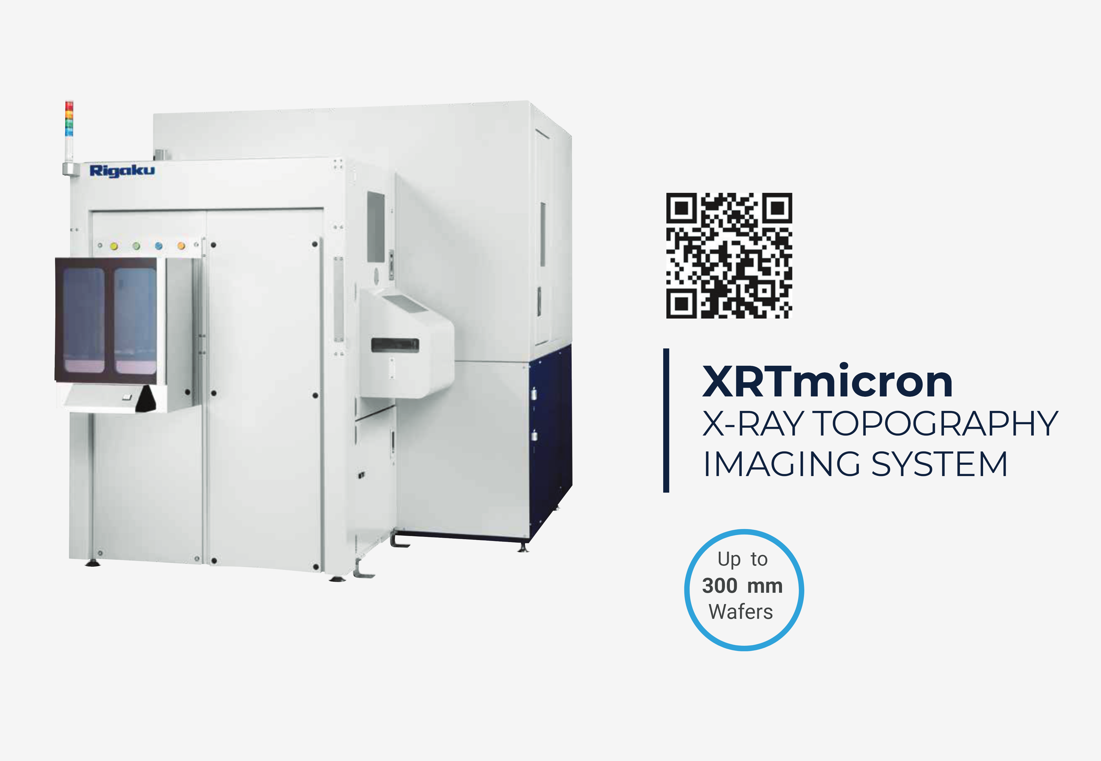
X-Ray Topography Imaging System
- High-brilliance dual-wavelength X-ray source: Micromax-007 DW
- High-resolution CCD camera: XTOP (5.4 μm pixels)
- Ultra-high resolution CCD camera: HR-XTOP (2.4 μm pixels)
- Horizontal sample mount for the minimum artificial strain to wafers
- Automatic wafer curvature correction for best dislocation image quality
- Automated system operation, including X-ray anode switch, detector switch, optics switch and sample alignment, and image collection
- Automated dislocation analysis 3, 4, 6, 8, 12-inch wafers supported
- Wafer loader compatible
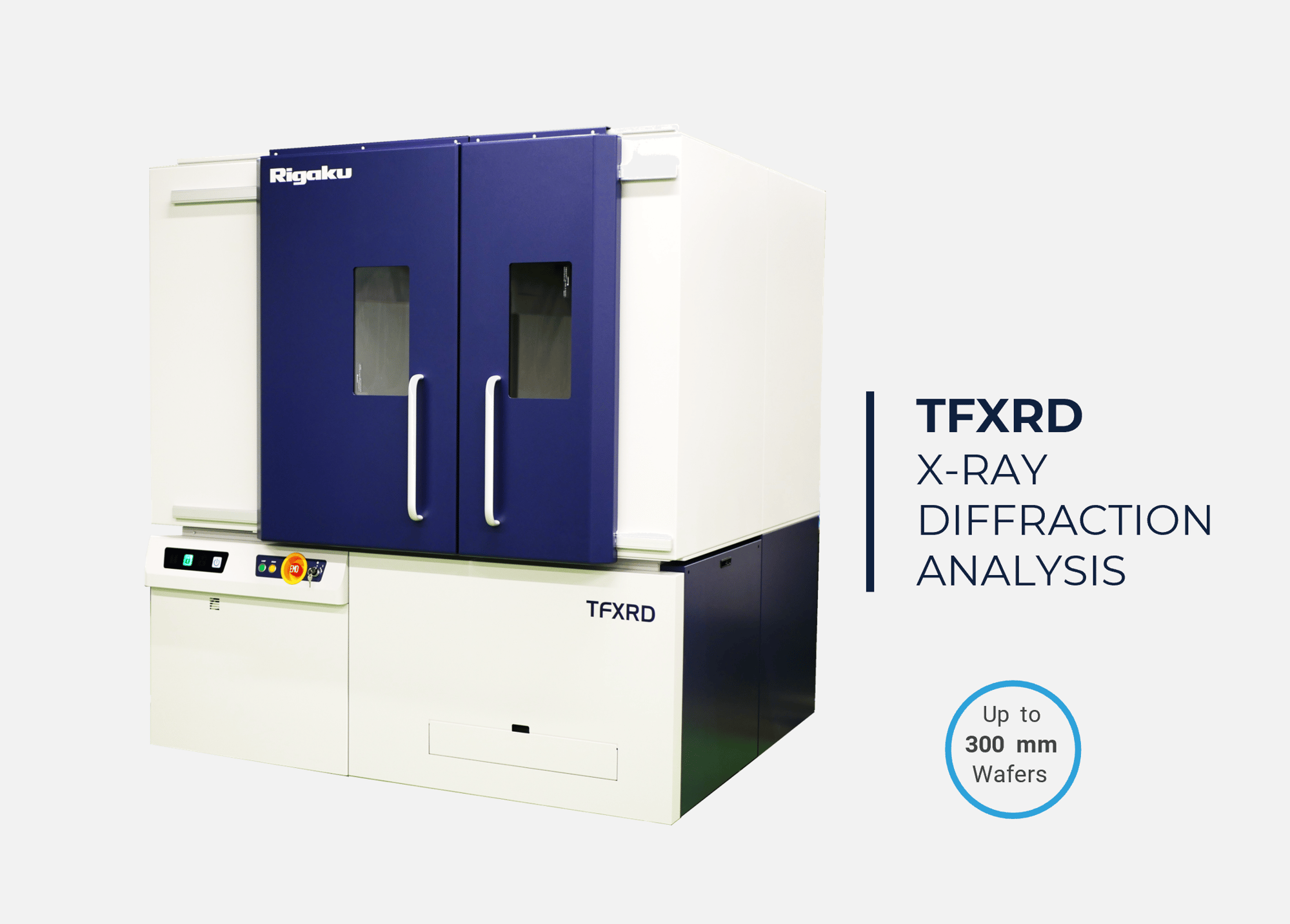
X-RAY DIFFRACTION ANALYSIS
NON-DESTRUCTIVE XRD SYSTEM MAPPING TOOL FOR NEAR-FAB APPLICATIONS
- Highest precision goniometer with selectable optics for all thin film XRD applications and XY-movable stage for mapping
- Efficient Measurement Speed
- Incident Monochromator for high-resolution measurements
- Large Wafer full-Mapping
- For up to 300 mm wafers
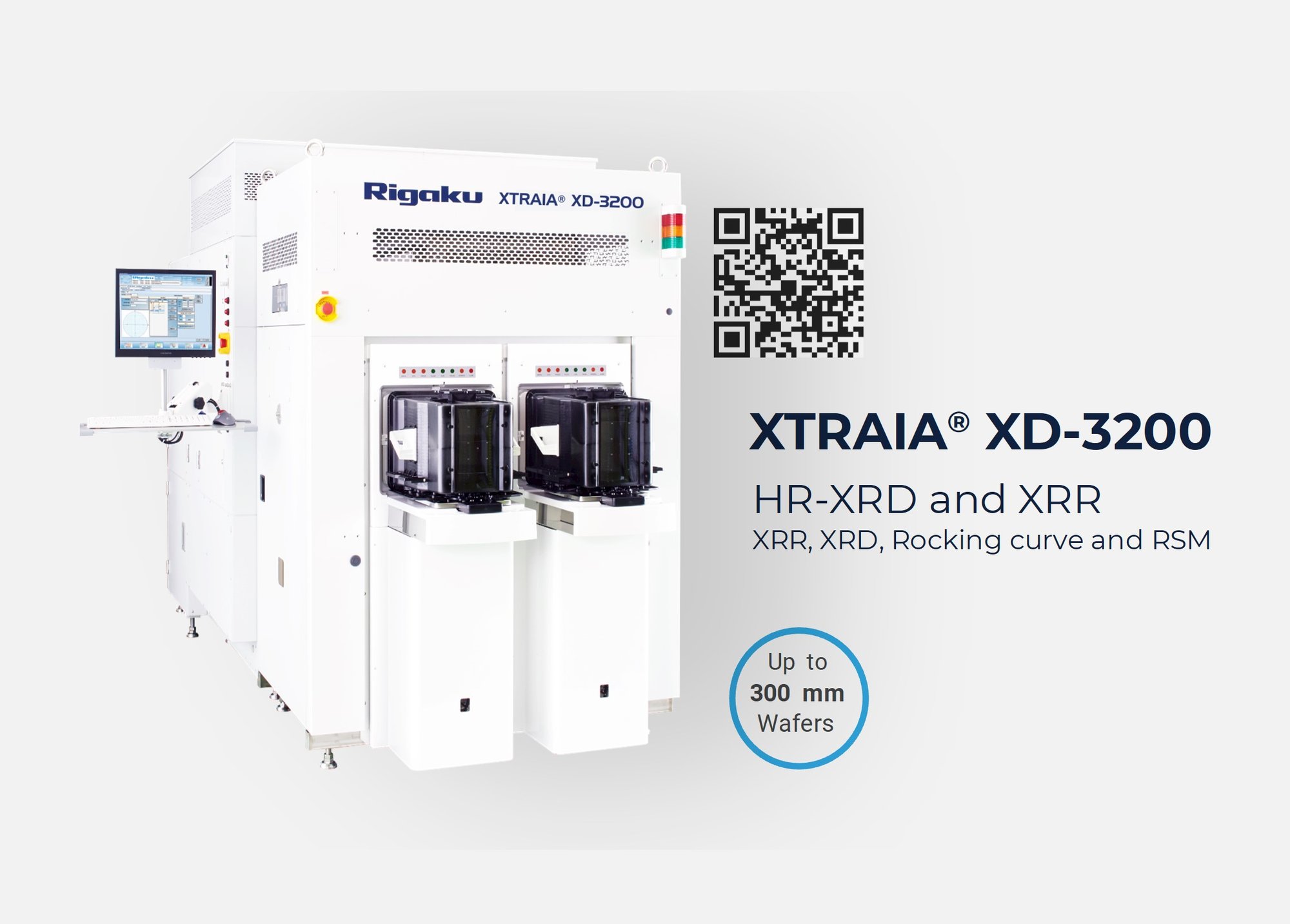
Blanket Epitaxial Thin Film
Si/SiGe Multilayer
- Non-destructive wafer analysis for multi-layered materials
- Epitaxial and polycrystalline films
- Measurements; thickness, composition, strain, relaxation, and structural quality
- 9 kW Rotating Anode or 2.2 kW Sealed XG Selectable
- X-ray Optics Line Focus With Mirror and/or 2/4 Bounce Crystal
- For Blanket wafers
- Cleanroom, in-line, fully automated GEM300 platform
- SEMI S2/S8 Compliant
CONTACT US
Rigaku Corporation
3-9-12, Matsubara-cho
Akishima-shi, Tokyo
196-8666, Japan
E-mail address info-gsm@rigaku.co.jp
Phone number +81 3-3479-0618
Rigaku Americas Corp.
9009 New Trails Drive
The Woodlands, TX
77381-5209, USA
E-mail address info@rigaku.com
Phone number +1-281-362-2300
Rigaku Europe SE
Hugenottenallee 167
Neu-Isenburg
63263 , Germany
E-mail address semieurope@rigaku.com
Phone Number +49 6102 77999 51
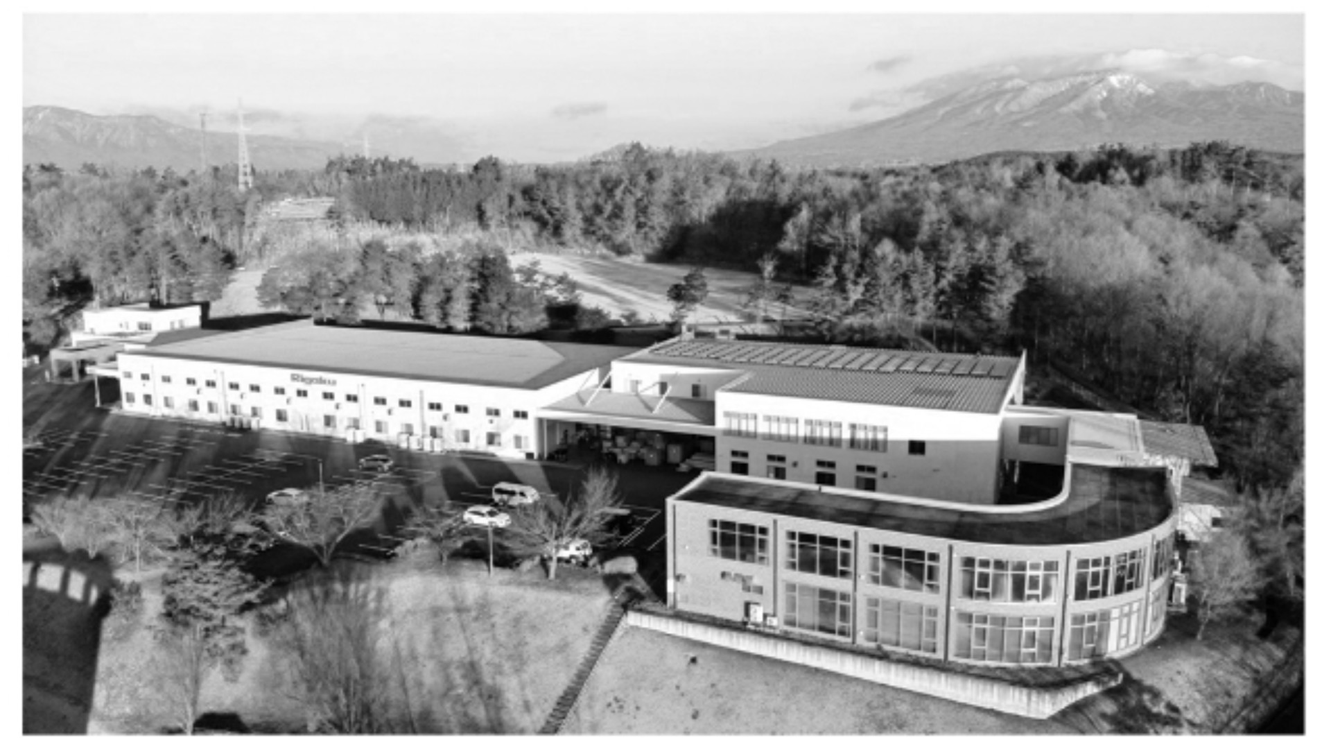
Rigaku Yamanashi Factory - Japan
Who we are
Rigaku Semiconductor Metrology Division
Semiconductors have the power to change the world for the better. Here at Rigaku, we strive to make this a reality as the leading global supplier of X-ray metrology tools for semiconductor process R&D and high-volume manufacturing.
CORPORATE MISSION
To contribute to the enhancement of humanity through scientific and technological development.
To contribute to the enhancement of humanity through scientific and technological development.
CORPORATE MOTTO
Value our customers, value our people, and value our technology.
Value our customers, value our people, and value our technology.
