WD-XRF APPLICATION
THICKNESS CHARACTERIZATION OF A POWER DEVICE
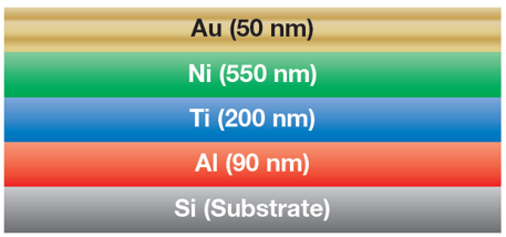
BACKSIDE ELECTRODE
WD-XRF can monitor metal film thickness and uniformity with high precision and throughput.
All four layers, even the bottom Al, can be analyzed simultaneously thanks to the high-power (4 kW) X-ray source and the FP method.

elements measeured by wd-xrf
| X Y | Au | Ni | Ti | Al |
| nm | nm | nm | nm | |
| Average (nm) | 49.3 | 551.3 | 198.2 | 89.5 |
| Maximun (nm) | 50.4 | 557.3 | 201.2 | 91.1 |
| Minimun (nm) | 48.1 | 544.8 | 195.3 | 87.9 |
| Range (nm) | 2.3 | 12.5 | 5.9 | 3.23 |
| Sigma (nm) | 0.90 | 3.59 | 1.61 | 0.87 |
| RSD (%) | 1.82 | 0.65 | 0.81 | 0.97 |

RECOMMENDED RIGAKU SEMICONDUCTOR METROLOGY TOOLS


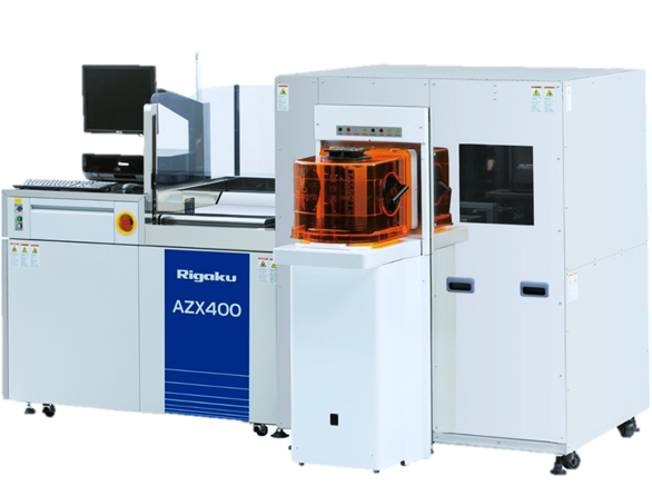
AZX 400
Sequential WDXRF spectrometer for elemental analysis and thin-film metrology of large and/or heavy samples
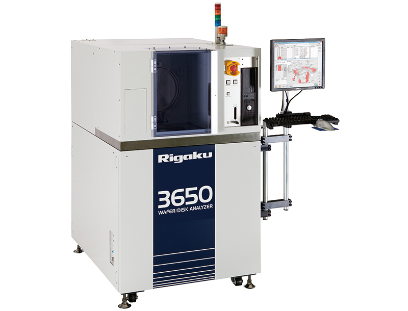
WDA-3650
Simultaneous WDXRF spectrometer for wafer metal film metrology; up to 200 mm wafers
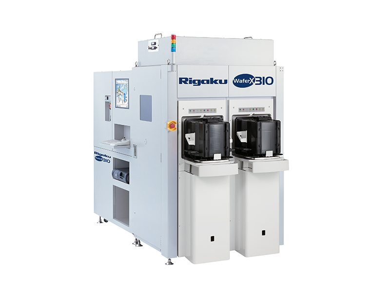
WAFERX 310
In-line, simultaneous WDXRF spectrometer for wafer metal film metrology; up to 300 mm wafers


