Rigaku Logo 100px
1417705_RSMDSemiconductorIcons_04_072122

ADVANCED PACKAGING APPLICATION

Pd Measurement on GaAs Wafer

Introduction


Gallium Arsenide (GaAs) wafers
The Gallium Arsenide (GaAs) wafers are next-generation technology, and the market is expected to grow at a CAGR of 12.5 percent between 2020 and 2025. GaAs is a more efficient substrate material than silicon and other compound semiconductors for making integrated-circuit chips because of better functionality, scalability, and compatibility with the IoT network.

Thanks to their superior properties, GaAs devices are expected to hold increasing share in various applications like mobile phones, satellite communications, microwave point-to-point links and higher frequency radar systems either in civil or military and space use.

Palladium (Pd)

Palladium is frequently used in the electronics industry as a plating for connectors and contacts. This is because of its low surface contact resistance. Often, a palladium-nickel alloy is plated on a connector surface before adding a flash of gold — this combination provides a low-cost, yet highly effective solution.


Problem Statement


GaAs wafers containing palladium present two major analytical problems:

  1. Palladium Kα overlaps with the arsenic sum peak. Arsenic is abundant everywhere in the wafer making it impossible to measure palladium Kα alone.

Pd Kα (eV)

As Sum Peak (eV)

21175

21080


  1. Palladium Lα overlaps with argon Kα. Argon is the third-most abundant gas in the atmosphere; therefore, present in every XRF spectrum.

Pd Lα (eV)

Ar Kα (eV)

2838

2957


Unique Solution

Elemental analysis and detection of low energies is performed with micro spots using the unique Onyx 3000 detector array, and by purging the air between the X-ray beam and sample using helium, which excludes argon from the measurement area. A controlled helium flow removes the argon from the area above the sample, resulting in a clear palladium Lα energy peak and allowing a precise measurement of the palladium thickness/concentration.

Using helium to purge argon from measurement area does not require a load lock chamber for vacuum, hence allowing measurement of large samples and improving throughput.


image-png-3
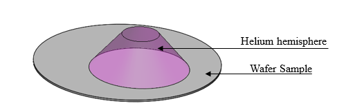
Figure 1: Onyx 3000 helium purge hemisphere demonstration


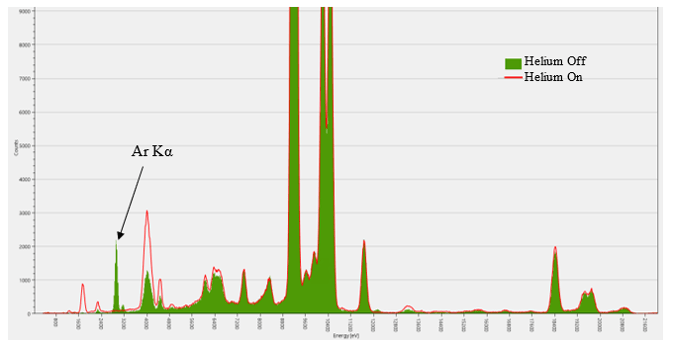
Figure 2: Background with and without the use of helium. The Ar peak disappears when using helium. 


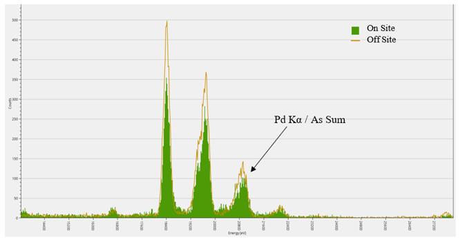
Figure 4: Spectrum zoom in at the Pd Kα/As sum peak energy line. On- and off-site Pd Kα ROI intensity is very similar due to the presence of As in the wafer.


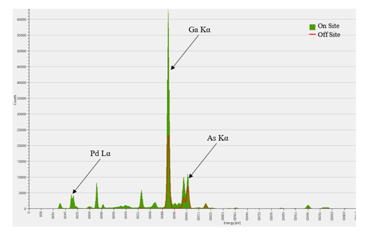
Figure 3: Typical spectra measured on and off a Pd-containing feature with helium purge. The off-site spectrum shows no Pd or Ar peaks.


Conclusion


This report shows the utilization of the micro-spot Onyx 3000 capabilities for measuring palladium on a GaAs sample using a unique detector array and helium purge to efficiently remove air (argon) from the X-ray path.

Compared to WDXRF technology, Onyx 3000 EDXRF uses micro spots down to 10 µm (depending on the sample material) versus 1-20 mm in most WDXRF tools. In addition, a load lock chamber for vacuum is not needed.

This method was tested and found to be highly effective for measuring palladium thickness or concentration on GaAs samples.


RECOMMENDED RIGAKU SEMICONDUCTOR METROLOGY TOOLS

BUMP INSPECTION SYSTEM

≤ 300 mm Metrology Solutions

ONYX 3000Hybrid metrology, XRF and optical x-ray, with  a 2D microscope, and 3D Scanner for blanket and patterned wafer thickness, composition, defect identification, and sizing


  • Hybrid Configuration
  • Micro-spot ED-XRF and 2D- and 3D- optical characterization of device structures
  • For FEOL, BEOL, and packaging applications
  • For up to 300 mm blanket and patterned wafers